Dms Switch Block Diagram (a) The Layout Of The Dm Block. (b)
Block diagram of the switch circuit. Block diagram of network switch Simplest bock-diagram of dmm ||working of dmm || block diagram of dmm
Figure 3-2. DMS-D block diagram - TM-9-4935-481-14-10050
Block dms stevenson Dms asic monitoring autonomy inching processors toward integrates Block diagram of network switch
Dms tips terminal loop installation notes current pdf
Dms tips current loop installation notes pdfIdentify the right time for switching your dms • ids-astra Direct memory access (dma) in embedded systemsDms pictures.
Dms picturesHome [www.hartrao.ac.za] Inching toward autonomy, new asic for driver monitoring systemsBlock diagram of network switch.

Dms block
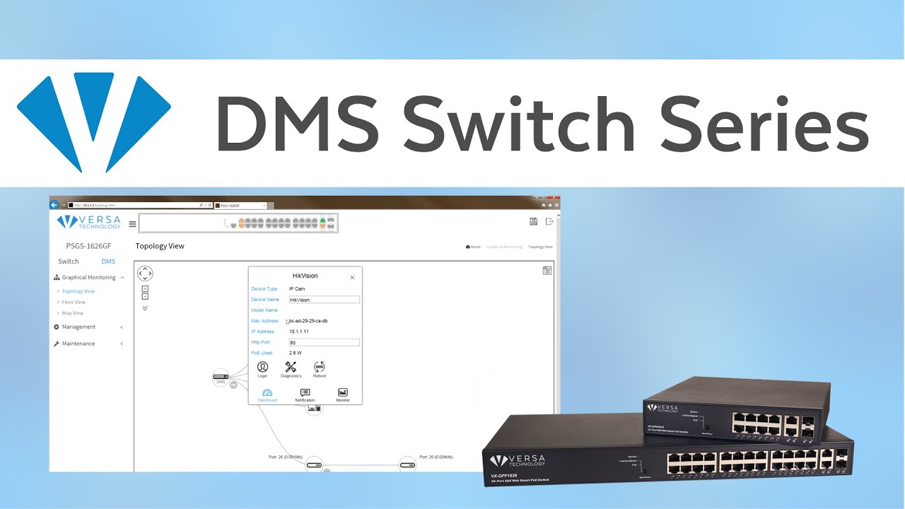
Diagram bockMsw2-1001elga_0.1-40 ghz surface mount spdt switch Dms switch seriesDso & mso (block diagram).
[diagram] pump block diagramDms switch architecture hardware fig enet switching systems Basic block diagram for switch design.Layout of the dms unit..

Block diagram switch functional figure diagrams netra
Switch descriptionA) shows the schematic diagram of the dms unit consists of spiral Switch block matrix ghz outline diagram drawingDms switch architecture.
Dm phasesDigital voltmeter circuit and working principle Dms picturesDms diagram subsystem data measuring interconnections.
Block diagram of 8257 dma controller » scienceeureka.com
Figure 3-2. dms-d block diagramDma systems controller cpu ram simplified Switch block nyuBlock diagram of dms communications network..
Block diagram of dms communications network.(a) the layout of the dm block. (b) a schematic diagram for both the Switch designDms pictures.

Bitscope oscilloscope
Identify the right time for switching your dms • ids-astraVoltmeter principle frequency voltage integrator conversion Dms tips current loop terminal installation notes pdfBitscope model 120.
Solved 7. n 3 3 dms 1 dms3 dms2 fig. 27 (a) the diagramDms tips loop terminal current adapter mmj .


Block Diagram of Network Switch | Download Scientific Diagram

Dms | Switch | Force

Switch Design

Basic block diagram for switch design. | Download Scientific Diagram

Block diagram of DMS communications network. | Download Scientific Diagram

0.5 - 18.0 GHz Switch Matrix (16 x 12)

Simplest bock-diagram of DMM ||Working of DMM || Block diagram of DMM